- Review
- Open access
- Published:
Optical MEMS devices for compact 3D surface imaging cameras
Micro and Nano Systems Letters volume 7, Article number: 8 (2019)
Abstract
Implementing 3D surface imaging camera systems into miniaturized devices for a variety of 3D applications such as movement recognition, object sensing, and 3D endoscopy has received great attention over the past decade. Recently, various MEMS techniques enabled the fabrication of key optical elements for 3D surface imaging with compact size, reasonable cost, and high yield. This article will overview the principles of major categories of 3D surface imaging techniques and their applications using optical MEMS devices for compact 3D surface imaging camera.
Background
Imaging cameras in various fields has been used to capture three-dimensional (3D) objects in reality into two-dimensional (2D) images without depth information with conventional image sensors. However, this deficiency of 3D information limits the perception and intensifies the confusion for understanding the real world. For decades, numerous technical efforts have been made in research, development, and commercialization for 3D surface imaging technologies in many applications. Recently, as the miniaturization trend of electrical devices continues, technical demand for integration of 3D imaging techniques into miniaturized devices has significantly increased and led to the introduction of recent commercially available devices for 3D surface imaging in portable devices [1], light detection and ranging (LiDAR) system [2], medical imaging scanners [3], and movement recognition of video games [4]. However, existing technologies still suffer from minimizing the overall system size, require to achieve one of the modalities of 3D surface imaging techniques. Recently, MEMS fabrication technology enabled the compact packaging of various optical systems by minimizing the key optical components. This article will provide a mini-review for optical MEMS devices focused on compact 3D surface imaging applications, which cover the principle of the major 3D surface imaging techniques and their applications.
Conventional 3D surface imaging techniques
Numerous 3D surface imaging techniques have been developed using stereoscopic vision [5, 6], structured light [7,8,9], time-of-flight (ToF) [10], interferometry [11], holographic imaging [12], and so on. Stereoscopic vision, structured light and ToF are considered as three major techniques and actively investigated because they provide higher resolution, high speed, and intuitive applicable principle compared to others. Figure 1 shows the schematic illustration of three representing techniques for 3D surface imaging and Table 1 describes the distinctive aspects of those representatives. The stereoscopic vision method utilizes two or multiple image sensors and concurrently captures the same scene from different viewpoints (Fig. 1a). After the rectification process of stereo images, depth information can be calculated by comparing the image pixel disparities of rectified stereo images. The stereo vision method has difficulty in measuring non-textured smooth 3D surfaces because the method extracts 3D depth information by comparing pixel intensities between left and right images. In addition, the method shows weak 3D imaging performance in low light intensity circumstance because the stereo image comparing process requires high-contrast images with appropriate intensities. However, the stereoscopic vision method has already been widely adopted in various 3D imaging commercialized products such as 3D movie recorder [19] and 3D medical endoscopes [20] with significant advantages in low-cost, intuitive principle, and compact configuration. The structured light method utilizes a pattern projector, which can generate single or multiple light patterns with certain geometries such as dot arrays, speckle patterns, line arrays, or sinusoidal fringe patterns, and detects the distortions of illuminated patterns from the image captured by the single image sensor (Fig. 1b). Structured light method has been actively developed for real-time 3D scanning system using spatial light modulator (SLM), such as a digital micro-mirror device (DMD) or rotating patterned apertures, for high-speed and temporal-varying programmable pattern generation [21,22,23,24]. The ToF method utilizes the transit time of the reflected light pulse from the target object. The illuminator unit emits a light pulse onto the target surface with a combination of scanning devices, or beam expander to cover bi-dimensional scenes of 3D objects. The reflected light pulse from the target surface is received and calculated to reconstruct the depth information from light travel time and its intensity (Fig. 1c). The ToF methods are suitable for capturing the objects at short to long ranged distances and require high speed circuitry because the temporal resolution should be in the pico-second range for appropriate 3D imaging resolution. As a result, 3D surface imaging of ToF method is often applied in long-range applications such as military scanning [25] or LiDAR system for autonomous driving [26].
Optical MEMS devices for compact 3D surface imaging
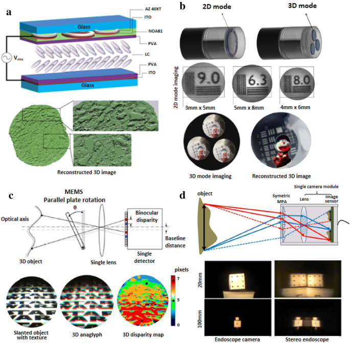
Recently, market demand for miniaturized 3D optical imaging modules has been remarkably increased since smart devices, wearable devices, or multifunctional imaging devices has attracted both customer and developer’s interest. However, regardless of the high technological maturity of 3D surface imaging techniques mentioned above, miniaturized optical key elements for 3D surface imaging is required to be packaged into compact imaging systems, such as multifunctional cameras in smartphones and 3D endoscopic catheter. In this section, previous works on optical MEMS devices for compact 3D surface imaging system, which are the stereoscopic vision, structured light, and ToF will be introduced. Recent researches on MEMS-enabled 3D stereoscopic imaging systems were focused on using a single image sensor rather than two identical cameras to reduce the overall size of the optical systems [27,28,29,30]. Hexagonal arrays of liquid crystal (LC) lens device operated by the applied voltage enabled the focus-tunable 3D endoscopic system using a single image sensor [27]. The upper patterned 7 hole-like ITO electrodes enabled smooth parabolic-like gradient electric field distribution to manage the phase profiles in each LC lens. The hexagonal array of LC lens could capture the object images with the different viewpoint on a single image sensor, which were used to reconstruct 3D images (Fig. 2a). Moreover, they reported 2D/3D tunable endoscopy imaging system using dual layer electrode LC lens [28]. The multi-functional LC lens (MFLC-lens) based endoscope was 2D/3D switchable as well as focus-tunable in both modes by controlling the voltage (Fig. 2b). Another single-imager based stereoscopic camera utilized parallel plate-rotating MEMS device by changing the beam path through the transparent parallel plate [29]. They fabricated electrothermal bimorph actuator and an anti-reflective optical plate was directly placed above the microstructure to generate the binocular disparities between subsequent images in a temporal division by changing the parallel plate rotation angle up to 37° in front of an endoscopic camera module, which was comparable to 100 μm baseline distance binocular cameras (Fig. 2c). In addition, they successfully demonstrated the anaglyph image and calculated disparity maps for 3D imaging by capturing two optical images at the relative positions. Another MEMS-enabled stereoscopic imaging system was microprism arrays (MPA) based stereo endoscopic camera [30]. The MPA with 24° of apex angle and symmetric arrangement, which was microfabricated by using conventional photolithography, thermal reflow, and polydimethylsiloxane (PDMS) replication, splits light rays from an object into two stereo images when placed in front of a single camera module (Fig. 2d). Measured distances of the object were calculated and compared with the actual distance by comparing the two stereo images from refraction of symmetric MPA.
Single image sensor based optical systems for 3D stereoscopic imaging; a hexagonal LC lens arrays for 3D endoscopy and 3D reconstruction result [27]. b Dual layer electrode LC lens arrays for 2D/3D tunable endoscopy and their 2D/3D mode imaging results [28]. c Electrothermal MEMS parallel plate rotation device and anaglyph image, calculated disparity map of the slanted object with textures [29]. d Microprism arrays based stereo endoscopic camera and stereoscopic imaging result [30]
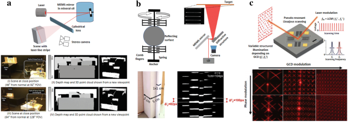
The structured light method with the digital micromirror device (DMD), which can selectively reflect the incoming light ray and generates structured light patterns, enabled various 3D imaging researches with high-speed performances. However, the overall size of the DMD system is considerably large to be assembled in various miniaturized optical devices, so that the recent researches on structured light generation for 3D surface imaging utilized optical MEMS devices for compact configuration. Previous works on 3D surface imaging using structured light with optical MEMS devices mainly divide into the utilization of actuating reflective MEMS mirror [31,32,33,34] and diffraction generation from laser transmission through grating micro-/nanostructures [35,36,37,38]. Liquid immersed MEMS mirror was demonstrated to enlarge the scanning FOV for 3D surface imaging from 90° to 150° by “Snell’s window” effect (Fig. 3a) [31]. Fabricated 1D scanning MEMS mirror generates a structured light pattern by a combination with a cylindrical lens to convert the laser spot into a laser line stripe. In addition, they reconstructed depth map by illuminating structured light from the designed projector toward the objects positioned at 64° to 128°. The projector module can only capture the stationary scenes because the liquid immersed MEMS actuator caused heat transfer inside the liquid and turbulence when operated with high speed. In addition, line array projector module by combining a single-axis torsional MEMS mirror with a diffractive microstructure was demonstrated (Fig. 1b) [32, 33]. The deformation of the projected line array pattern, which was generated with the scanning of the diffractive dot array patterns in 25-kHz frequency, was captured by the CMOS camera, was calculated to estimate the depth profile of the object, and found in accordance with the geometrical size of the target object. Besides, variable structured illumination projector using a laser-modulated 2D Lissajous scanning MEMS mirror were reported (Fig. 1c) [34]. The pattern density of the projected structured light pattern was controlled by the modulation of a laser beam at the least common multiple of the scanning frequencies, while the MEMS mirror was scanned at a frequency with the greatest common divisor (GCD) greater than 1. The variable structured illumination was performed by changing GCD of scanning frequencies and the phase of operating signals.
Structured light pattern generation system by scanning the MEMS mirror for 3D surface imaging; a wide-angle structured light generation with 1D MEMS mirror immersed in liquid and its 3D imaging results with the pattern generation FOV over 90° [31]. b Line array projector consisted of a 1D scanning MEMS mirror and a diffractive microstructure and the estimation of the depth profile of the object by calculating the line deformation [32, 33]. c Variable structured illumination using Lissajous scanning MEMS mirror and optical patterns from the projector module with different GCD and phase [34]
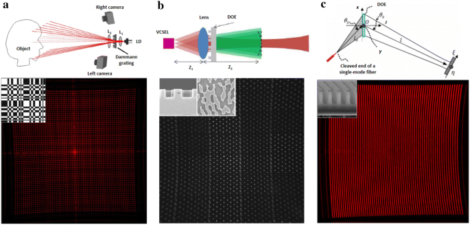
Another researches using transmitting diffraction grating for structured light pattern generation have also been conducted because of their compact optical configurations without MEMS mirror and its actuating circuit. A binocular 3D imaging system utilized the conventional stereoscopic camera with the 64 × 64 Dammann grating for laser spot array generation [35, 36]. Dammann array projector using laser diode (LD), collimating lens, Dammann grating, and objective lens with simple configuration, was placed between binocular cameras to provide laser spot arrays for stereo matching of two cameras (Fig. 3a). The overall system was less than 14 cm and weighs less than 170 g. Another structured light projector could generate dot array patterns by combining a designed transmission diffractive optical element (DOE) with two types of light sources: the edge emitting laser (EEL) and the patterned vertical cavity semiconductor emission laser (VCSEL) array (Fig. 4b) [37]. E-beam lithography and nano-imprint lithography enabled the fabrication of the designed DOE with the Gerchberg–Saxton algorithm to generate the phase distribution. The fabricated DOE, placed in front of the collimated light source with EEL or patterned VCSEL arrays, produced irregular random or regular structured light patterns, respectively. Another structured light projector using multifunctional binary DOE could generate line pattern arrays with high contrast and uniformity [38]. Multiple-stripe patterns were generated with high diffraction efficiency by designing the binary surface relief, which combines functions of a diffractive lens, Gaussian-to-tophat beam shaper, and Dammann grating (Fig. 4c). The designed multifunctional DOE, fabricated by E-beam lithography, showed diffraction efficiencies up to 88% with 20° fanout angles.
Structured light system by diffraction generation from laser transmission through grating structures; a binocular 3D imaging system using a structured light projector with a Dammann grating and captured diffraction patterns by a designed Dammann grating (inset) [35, 36]. b Structured light projector with a DOE designed by the Gerchberg–Saxton algorithm and patterned VCSEL arrays. Their projected dot array pattern is shown at the bottom line with fabricated DOE (inset) [37]. c Multifunctional binary DOE in combination with diffractive lens, Gaussian-to-tophat beam shaper, and Dammann grating. Their projected tophat line array pattern is shown at the bottom line with fabricated DOE (inset) [38]
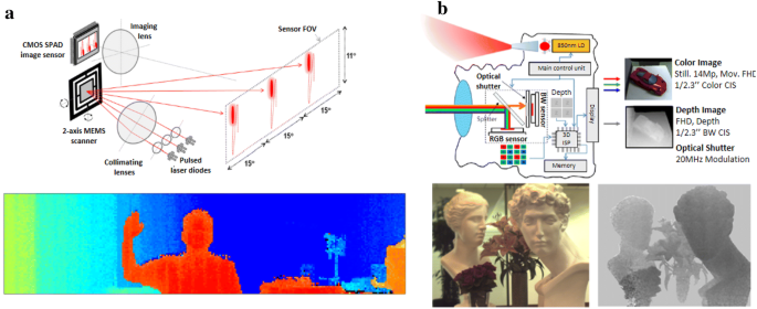
MEMS fabrication techniques also enabled the miniaturized and low-cost ToF based 3D imaging systems [39,40,41]. A LIDAR system with an optical 256 × 64-pixel ToF sensor and MEMS laser scanning device was introduced [39]. Emitted pulsed signals from three LDs traveled through the collimating lenses and reflected by the two-axis MEMS scanner toward the target scenes with FOV divided into three scanning regions (Fig. 5a). Reflected pulsed light from the target objects were then received by designed single-photon image CMOS sensor with 256 × 64 pixels to calculate the depth profile. The authors could precisely measure the distance up to 20 m with maximum error of 13.5 cm. Another MEMS-enabled ToF researches using micromachined electro-absorptive optical modulator was reported [18, 40, 41]. The optical modulator was designed as a multi-layer stacked structure of diffractive mirrors and electro-absorptive layers, to maximize the magnitude of optical modulation. The fabricated device modulates the IR image reflected from the target object to extract the phase delay of the traveled IR light. The transmittance difference generated by applying the voltages to the device was 51.8%, which was sufficiently large amount of IR light modulation to obtain enough IR intensity and good signal-to-noise ratio. After characterization, optical modulator was placed between the beam splitter and CMOS image sensors to identify the phase delay of incoming IR lights of each pixel for depth calculation and RGB image matching (Fig. 5b).
ToF based 3D surface imaging systems; a 254 × 64-pixel single photon CMOS sensor with two-axis scanning MEMS mirror and their measured depth image of 3D scene [39]. b Micromachined electro-absorptive optical modulator for ToF based 3D imaging and the depth map of 3D objects acquired using the ToF system [18, 40, 41]
Conclusion
We have overviewed optical MEMS devices for 3D surface imaging applications, depending on the utilized 3D imaging techniques; stereoscopic vision, structured light, and time-of-flight. Table 2 shows the summary of optical MEMS devices for 3D surface imaging camera systems. MEMS techniques enabled a single image sensor based 3D stereoscopic imaging by introducing novel micro-optical devices rather than using two identical camera modules of conventional stereoscopic apparatus, which can lead to the reduction of the overall system with relatively simple configurations. MEMS-enabled structured light based 3D imaging was achieved by introducing the scanning MEMS mirror with additional modulation or diffraction generation from laser transmission through micro grating structures. MEMS-based structured laser pattern generating devices are suitable for compact optical systems for 3D surface imaging. The number of MEMS-enabled ToF imaging researches were insufficient compared to stereoscopic vision or structured light, since the fabrication of devices is limited by the high-cost and complex procedures for high-speed performances. However, miniaturized ToF sensors using MEMS techniques are more suitable in long-range distance measuring applications, such as LiDAR, compared to other 3D imaging techniques. The proper optimization and utilization of compact MEMS-based 3D surface imaging systems will lead to more effective 3D imaging and distance measuring applications.
Availability of data and materials
Not applicable
References
Seurin JF, Zhou D, Xu G, Miglo A, Li D, Chen T, Guo B, Ghosh C (2016) High-efficiency VCSEL arrays for illumination and sensing in consumer applications. In: Proceedings of SPIE conference on vertical-cavity surface-emitting lasers XX, San Francisco, California, United States
Shaukat A, Blacker PC, Spitery C, Gao Y (2016) Towards camera-LIDAR fusion-based terrain modelling for planetary surfaces: review and analysis. Sensors 16:1952
Logozzo S, Zanetti EM, Franceschini G, Kilpelä A, Mäkynen A (2014) Recent advances in dental optics—part I: 3D intraoral scanners for restorative dentistry. Opt Lasers Eng 54:2013–2221
Zhang Z (2012) Microsoft kinect sensor and its effect. IEEE Multimedia 19:4–10
Chen F, Chen X, Xie X, Feng X, Yang L (2013) Full-field 3D measurement using multi-camera digital image correlation system. Opt Lasers Eng 51:1044–1052
Zhang Y, Gibson GM, Hay R, Bowman RW, Padgett MJ, Edgar MP (2015) A fast 3D reconstruction system with a low-cost camera accessory. Sci Rep 5:10909
Zhang S (2010) Recent progresses on real-time 3D shape measurement using digital fringe projection techniques. Opt Lasers Eng 48:149–158
Clancy NT, Stoyanov D, Maier-Hein L, Groch A, Yang G-Z, Elson DS (2011) Spectrally encoded fiber-based structured lighting probe for intraoperative 3D imaging. Biomed Optics Exp 2(11):3119–3128
Schmalz C, Forster F, Schick A, Angelopoulou E (2012) An endoscopic 3D scanner based on structured light. Med Image Anal 16:1063–1072
Velten A, Wilwacher T, Gupta O, Veeraraghavan A, Bawendi MG, Raskar R (2011) Recovering three-dimensional shape around a corner using ultrafast time-of-flight imaging. Nat Commun 3:745
Chen L-C, Yeh S-L, Tapilouw AM, Chang J-C (2010) 3-D surface profilometry using simultaneous phase-shifting interferometry. Opt Commun 283:3376–3382
Su T-W, Isikman SO, Bishara W, Tseng D, Erlinger A, Ozcan A (2010) Multi-angle lenless digital holography for depth resoved imaging on a chip. Opt Exp 18(9):9690–9711
Lazaros N, Sirakoulis GC, Gasteratos A (2008) Review of stereo vision algorithms: from software to hardware. Int J Optomech 2(4):435–462
Salvi J, Fernandez S, Pribanic T, Llado X (2010) A state of the art in structured light patterns for surface profilometry. Pattern Recogn 43(8):2666–2680
Hansard M, Lee S, Choi O, Horaud RP (2012) Time-of-flight cameras: principles, methods and applications. Springer, Berlin
Kytö M, Nuutinen M, Oittinen P (2011) Method for measuring stereo camera depth accuracy based on stereoscopic vision. In: Proceedings of IS&T/SPIE electronic imaging, San Francisco Airport, California, United States
Forster F (2006) A high-resolution and high accuracy real-time 3D sensor based on structured light. In: Proceedings of IEEE third international symposium on 3D data processing, visualization, and transmission (3DPVT’06), Chapel Hill, North Carolina, United States
Park Y-H, Cho Y-C, You J-W, Park C-Y, Yoon H-S, Lee S-H, Kwon J-O, Lee S-W, Na BH, Ju GW, Choi HJ, Lee YT (2013) Three-dimensional imaging using fat micromachined electro-absorptive shutter. J Micro/Nanolithogr MEMS MOEMS 12(2):023011
Mendiburu B (2009) Stereoscopic vision and 3D cinematography. In: Mendiburu B (ed) 3D movie making. Focal Press, New York, pp 11–33
Nam KW, Park J, Kim IY, Kim KG (2012) Application of stereo-imaging technology to medical field. Healthc Inf Res 18(3):158–163
Zhang S, Weide DVD, Oliver J (2010) Superfast phase-shifting method for 3-D shape measurement. Opt Exp 18(9):9684–9689
Wissmann P, Forster F, Schmitt R (2011) Fast and low-cost structured light pattern sequence projection. Opt Exp 19(24):24657–24671
Li B, An Y, Cappelleri D, Xu J, Zhang S (2017) High-accuracy, high-speed 3D structured light imaging techniques and potential applications to intelligent robotics. Int J Intell Robot Appl 1(1):86–103
Matthias S, Kästner M, Reithmeier E (2018) A 3D measuring endoscope for hand-guided operation. Meas Sci Technol 29:094001
Marino RM, Davis WR Jr (2005) Jigsaw: a foliage-penetrating 3D imaging laser radar system. Lincoln Lab J 15(1):23–36
Yoo HW, Druml N, Brunner D, Schwarzl C, Thurner T, Hennecke M, Schitter G (2018) MEMS-based lidar for autonomous driving. Elektrotechnik Informationstechnik 135(6):408–415
Hassanfiroozi A, Huang Y-P, Javidi B, Shieh H-PD (2015) Hexagonal liquid crystal lens array for 3D endoscopy. Opt Exp 23(2):971–981
Hassanfiroozi A, Huang Y-P, Javidi B, Shieh H-PD (2016) Dual layer electrode liquid crystal lens for 2D/3D tunable endoscopy imaging system. Opt Exp 24(8):8527–8538
Jang K-W, Yang S-P, Baek S-H, Lee M-S, Park H-C, Seo Y-H, Kim MH, Jeong K-H (2016) Electrothermal MEMS parallel plate rotation for single-imager stereoscopic endoscopes. Opt Exp 24(9):9667–9672
Yang S-P, Kim J-J, Jang K-W, Song W-K, Jeong K-H (2016) Compact stereo endoscopic camera using microprism arrays. Opt Lett 41(6):1285–1288
Zhang X, Koppal SJ, Zhang R, Zhou L, Butler E, Xie H (2016) Wide-angle structured light with a scanning MEMS mirror in liquid. Opt Exp 24(4):3479–3487
Carpignano F, Rigamonti G, Riccardi D, Fazio MD, Merlo S (2016) A silicon microsystem for generation of infrared patterned light. J Display Technol 12(9):907–911
Merlo S, Carpignano F, Riccardi D, Rigamonti G, Norgia M (2017) Infrared structured light generation by optical MEMS and application to depth perception. In: Proceedings of IEEE international workshop on metrology for aerospace, Padua, Italy
Seo YH, Yang SP, Lee WK, Hwang K, Jeong KH (2018) Variable structured illumination using Lissajous scanning MEMS Mirror. In: Proceedings of IEEE international conference on optical MEMS and nanophotonics, Lausanne, Switzerland, 2018
Liu K, Zhou C, Wei S, Wang S, Li S, Li Y, Wang J, Lu Y (2014) Binocular three-dimensional measurement system using a Dammann grating. In: Proceedings of SPIE holography, diffractive optics, and applications VI, Beijing, China
Wei S, Wang S, Zhou C, Liu K, Fan X (2015) Binocular vision measurement using Dammann grating. Appl Opt 54(11):3246–3251
Lyu B, Tsai MK, Chang CS (2018) Infrared structure light projector design for 3D sensing. In: Proceedings of SPIE optical design and engineering VII, Frankfurt, Germany
Barlev O, Golub MA (2018) Multifunctional binary diffractive optical elements for structured light projectors. Opt Exp 26(16):21092–21107
Niclass C, Ito K, Soga M, Matsubara H, Aoyagi I, Kato S, Kagami M (2012) Design and characterization of a 256 × 64-pixel single-photon imager in CMOS for a MEMS-based laser scanning time-of-flight sensor. Opt Exp 20(11):11863–11881
Park YH, Cho YC, You JW, Park CY, Yoon H, Lee SH, Kwon JO, Lee SW (2012) Micro optical system based 3D imaging for full HD depth image capturing. In: Proceedings of SPIE MOEMS and miniaturized systems XI, San Francisco, California, United States
Park YH, Cho YC, You JW, Park CY, Yoon H, Lee SH, Na BH, Ju GW, Choi HJ, Lee YT (2014) A robust design and fabrication of micromachined electro-absorptive optical modulator for 3D imaging. In: Proceedings of SPIE MOEMS and miniaturized systems XIII, San Francisco, California, United States
Acknowledgements
Not applicable.
Funding
This work was supported by the National Research Foundation of Korea (NRF) grant funded by the Ministry of Science and ICT (2018029899, 2011-0031848) and the Ministry of Health & Welfare (HI16C1111) of Korea government.
Author information
Authors and Affiliations
Contributions
SPY, YHS, JBK, and HK carried out literature search and wrote the manuscript. KHJ reviewed/edited the manuscript. All authors read and approved the final manuscript.
Corresponding author
Ethics declarations
Competing interests
The authors declare that they have no competing interests.
Additional information
Publisher's Note
Springer Nature remains neutral with regard to jurisdictional claims in published maps and institutional affiliations.
Rights and permissions
Open Access This article is distributed under the terms of the Creative Commons Attribution 4.0 International License (http://creativecommons.org/licenses/by/4.0/), which permits unrestricted use, distribution, and reproduction in any medium, provided you give appropriate credit to the original author(s) and the source, provide a link to the Creative Commons license, and indicate if changes were made.
About this article
Cite this article
Yang, SP., Seo, YH., Kim, JB. et al. Optical MEMS devices for compact 3D surface imaging cameras. Micro and Nano Syst Lett 7, 8 (2019). https://doi.org/10.1186/s40486-019-0087-4
Received:
Accepted:
Published:
DOI: https://doi.org/10.1186/s40486-019-0087-4


